What is the shielding net of LCD screen?

The shielding mesh (also known as EMI shielding mesh, conductive cloth/foam) of LCD screen is a conductive layer or wrapping material used to suppress electromagnetic interference, usually metal wire mesh, conductive cloth, conductive foam or metal foil,
The shielding mesh (also known as EMI shielding mesh, conductive cloth/foam) of LCD screen is a conductive layer or wrapping material used to suppress electromagnetic interference, usually metal wire mesh, conductive cloth, conductive foam or metal foil, located on the back or around the LCD module.
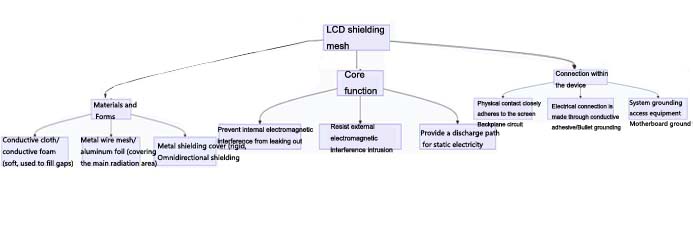
Its core function is to form a Faraday cage, ensuring that the electromagnetic waves generated by the high-speed circuit inside the screen do not leak out, while preventing external electromagnetic waves from interfering with the normal operation of the screen. The following figure shows the typical position and material composition of the shielding mesh in the LCD module
And its electrical connection principle in the whole machine:

The main forms and locations of blocking nets
1. Structural form:
Conductive cloth/foam: the most common, soft and elastic, often with adhesive backing, used to fill gaps and wrap cables.
Metal wire mesh/aluminum foil: covering the screen back panel or driver chip.
Integrated metal shielding cover: a metal cover that covers the entire logic board.
2. Installation location:
Screen back: Covering the entire metal backplate or logic board area.
Surrounding the cable: Wrap high-speed signal cables such as LVDS/EDP.
Inside the screen frame: Ensure good conductive contact between the module and the metal casing.
Key design points and grounding
Shielding nets must be effectively grounded to function, usually through the following methods:
Conductive adhesive/foam: pressed between the screen back panel and the metal casing/bracket of the device.
Metal shrapnel: Connect the shielding mesh to the ground wire (GND) of the device motherboard.
Direct soldering: Solder the shielding layer onto the grounding pad of the PCB.
Poor grounding is the most common cause of shielding failure, which can lead to increased interference.
The significance of design and maintenance
For designers, physical contact space and reliable grounding paths must be reserved for the shielding net during structural design. This is the key to the product passing EMC (Electromagnetic Compatibility) certification (such as CE, FCC).
For repairers: After replacing the screen or disassembling the device, it is necessary to restore the original shielding layer and not discard or omit it at will, otherwise it may cause the device to interfere with other components (such as Wi Fi, cellular antenna) or display abnormalities.
Simply put, the shielding mesh of the LCD screen is the "invisible guardian" that ensures display stability and equipment electromagnetic compliance. It is directly related to the integrity of LVDS/eDP high-speed signals that we previously discussed, as signal radiation is the main source of interference.
If you encounter specific display interference issues in the device or have deeper questions about EMC design, you can provide more details for further exploration.
AU Industrial LCD Screen:https://www.idtdisplay.com/products/AUO_LCD_Displays/